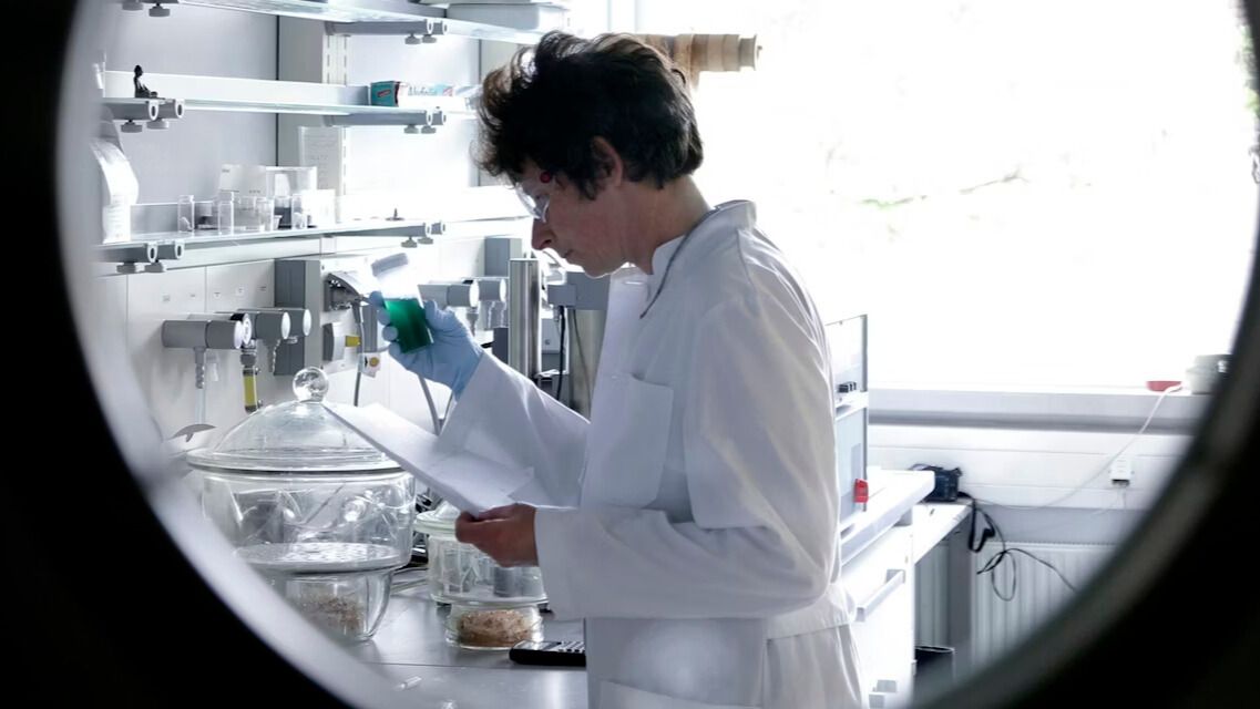
Materials engineers at Stanford University have introduced a significant advancement in infrared technology by employing a centennial semiconductor material. Their research, detailed in two recent papers, offers a new methodology aimed at enhancing infrared light-emitting diodes (LEDs) and sensors. This innovative approach promises to streamline production, leading to smaller, more efficient, and cost-effective infrared devices for various applications.
The semiconductor in question has been a staple in electronics for over a century. Despite extensive research in the field, breakthroughs involving semiconductors have become increasingly rare. The team at Stanford has managed to breathe new life into this well-established material, opening avenues for its application in critical sectors, including environmental monitoring, medical diagnostics, and industrial processes.
One of the standout features of this new approach is its potential to significantly reduce the size and costs associated with infrared technologies. Traditional infrared devices often face limitations related to bulkiness and production expenses, which can hinder their widespread adoption. By reimagining the use of a familiar semiconductor, the Stanford engineers aim to overcome these obstacles and enhance the functionality of infrared devices.
The implications of this research extend beyond mere technical specifications. Improved infrared sensors and LEDs can play a crucial role in environmental science by facilitating real-time monitoring of pollutants and climate change indicators. In the medical field, these advancements could lead to more accurate diagnostic tools, enhancing patient care. Furthermore, industries relying on infrared technology could benefit from increased efficiency and reduced operational costs.
Research lead Dr. Emily Chen, a materials engineer at Stanford, emphasized the importance of this development. “By leveraging a material with proven capabilities, we can break new ground in infrared technology,” she stated, highlighting the research’s potential to impact a broad spectrum of industries.
The two papers published by the Stanford team have already garnered attention from the scientific community. Experts are keen to see how this innovative application of a century-old material will influence future research and development in semiconductor technology. The expectations are high, with many anticipating that these advancements could reshape the landscape of infrared applications.
As the world continues to seek innovative solutions for pressing challenges, the work at Stanford serves as a reminder of the value of revisiting established technologies. By rethinking how existing materials can be utilized, engineers are paving the way for significant advancements that could lead to safer, more efficient technologies across numerous fields.
The Stanford engineers’ findings underscore the potential for further exploration in semiconductor applications, encouraging ongoing research and collaboration within the industry. This breakthrough not only enhances the existing capabilities of infrared devices but also sets the stage for future innovations that could emerge from the intersection of traditional materials and modern technology.